China's IMECAS Achieves GAA Transistors Without EUV, But 3nm Production Remains Years Away
Researchers at China's Institute of Microelectronics have successfully fabricated working gate-all-around transistors using only DUV lithography, sidestepping the need for Western EUV tools, though a commercially viable 3nm process is still distant.
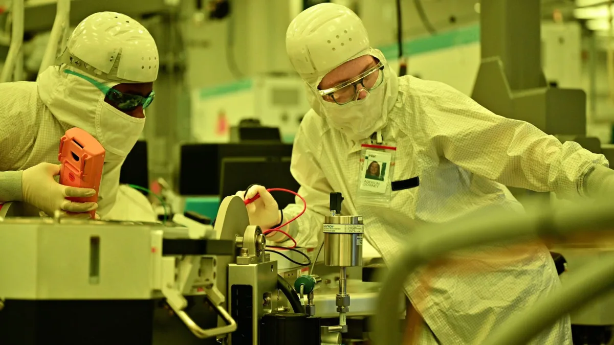
The Institute of Microelectronics of the Chinese Academy of Sciences (IMECAS) has created an experimental process for manufacturing stacked-nanosheet gate-all-around (GAA) transistors using immersion DUV lithography, producing functional devices in the process. This technique is being developed for potential deployment in 3nm-class and smaller nodes by Chinese semiconductor manufacturers lacking access to EUV scanners, according to DigiTimes.
Despite IMECAS's success in demonstrating working GAA devices, the organization has withheld disclosure of essential geometric specifications needed to assess how these transistors compare to 3nm-class offerings from competitors. The experimental process flow represents early-stage research rather than a finalized manufacturing procedure suitable for production chips, let alone a complete 3nm-class technology platform.
The breakthrough carries significant implications, showing that China possesses the capability to advance its semiconductor technology independently without relying on cutting-edge equipment sourced from Western suppliers.
Early process integration complete
At the IC World conference in Beijing, Ye Tianchun, chief engineer overseeing China's National Major Special Project 02, announced that IMECAS had finished 'early process integration' for stacked nanosheet-channel GAA transistors produced using DUV lithography. The IMECAS team achieved Ion/Ioff ratios of 9.7×10⁵ and 7.6×10⁵, both surpassing the 5×10⁵ benchmark, confirming that gate control of the stacked sheets functions properly. These measurements demonstrate that the experimental transistors successfully switch between conducting and non-conducting states, though they provide minimal insight into transistor density or whether physical dimensions align with specifications expected from commercial 3nm-class processes.
Notably, IMECAS has refrained from publishing gate pitch, metal pitch, nanosheet dimensions, transistor density, SRAM density, or other geometric data that would enable meaningful comparison against 3nm-class production nodes from Intel, Samsung Foundry, or TSMC. The work should therefore be interpreted as proof-of-concept for a stacked-nanosheet GAA process utilizing DUV lithography, rather than confirmation that China has engineered a functional 3nm process independent of EUV technology.
The core significance lies in IMECAS's exploration of how GAA devices intended for future 3nm-class and more advanced generations can be manufactured without EUV lithography—a feat not previously accomplished in volume production.
GAA transistors have displaced FinFET designs at cutting-edge nodes because wrapping the gate around nanosheet channels delivers superior electrostatic control as transistor sizes contract. IMECAS commenced work on these technologies in 2020, concentrating particularly on nodes below 3nm, which explains the organization's current emphasis on 3nm in its public statements.
Reducing China's dependence on advanced foreign tools
IMECAS's recent efforts have centered on diminishing China's reliance on tools, software, and technologies originating from Western companies and therefore vulnerable to export controls imposed by the United States, Japan, or Europe.
Ye highlighted architectural innovation, design-technology co-optimization (DTCO), system-technology co-optimization (STCO), and "extracting more value" from mature fabrication technologies as key focus areas. Currently, IMECAS's accomplishment illustrates a DUV-based pathway for investigating stacked-nanosheet GAA transistors destined for future 3nm-class nodes, but it does not represent a China-developed 3nm technology prepared for manufacturing in any foreseeable timeframe.
Even if IMECAS subsequently demonstrates appropriately scaled GAA devices employing DUV or releases critical geometry specifications from its current research, this would still fall far short of production-ready 3nm-class technology. Viable commercial manufacturing demands integration of lithography with deposition, etching, cleaning, metrology, process control, materials, temperature management, and numerous additional steps and parameters. At present, IMECAS has not demonstrated such a comprehensive manufacturing flow.